Concept → Campus
Company formed; PIMC concept developed; state / location, technology and OEM partners selected; government approvals and incentives pursued.


Energy • Materials • Semiconductors
PowerIn Urja is developing an integrated manufacturing campus designed to strengthen India's clean-tech and semiconductor supply chains — beginning with advanced N-Type solar ingot and wafer manufacturing.

PowerIn Integrated Manufacturing Campus · Nagpur, Maharashtra
Green powered
100% green-energy ambition
Upstream
Critical ingot & wafer node
3-phase campus
Solar • Semiconductor • Advanced devices
The thesis
PowerIn Urja's strategy is to create domestic manufacturing capability at the most structurally constrained points of the energy-transition and technology value chain. The platform is designed to move from Solar critical materials into Semiconductor, Neocloud, Storage, Hydrogen, Photonics and Mechatronics opportunities over time.
300+
acre campus vision
6 GW
Phase I ingot & wafer platform
3
phased development roadmap
Why it matters
Focuses on ingots and wafers — the upstream layer on which downstream solar cell and module manufacturing depends.
Czochralski mono-crystal growth and Tungsten-wire wafering are aligned to TOPCon, HJT and next-generation tandem-compatible products.
Campus infrastructure is intended to support future semiconductor, energy storage, hydrogen, photonics and mechatronics programmes.
About the campus
PowerIn Urja India Private Limited (PIU) is developing the PowerIn Integrated Manufacturing Campus (PIMC) at MIDC Additional Butibori, Nagpur, Maharashtra. The wider campus is planned across 300+ acres, with Phase I focused on advanced solar ingot and wafer manufacturing.
The platform is conceived to span a value chain from hyper-pure polysilicon, solar and semiconductor ingots / wafers through devices and critical consumables, neocloud, energy storage, hydrogen-based devices, photonics, mechatronics and selected ancillaries and R&D.
300+ acres
planned campus
6 GW
N-Type Ingot + Wafer
250,000 wafers
Semiconductor pilot line + Neocloud
Company formed; PIMC concept developed; state / location, technology and OEM partners selected; government approvals and incentives pursued.
Government approvals and incentive framework secured; equity commitments and strategic supply / offtake arrangements established; Phase-I implementation underway.
Phase II implements semiconductor ingot & wafer capacity and introduces semiconductor MiniFAB capability, Hyper-pure polysilicon, expanded energy storage and next-generation solar technology.
Further expansion of existing capacities and introduction of additional product lines based on business case and technology readiness.
Project at a glance
Phase I · 6 GW platform
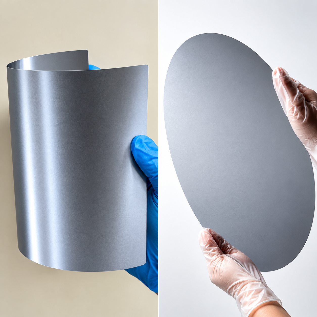
State-of-the-art Czochralski mono-crystal growth combined with Tungsten-wire wafering, compatible with PERC, TOPCon, HJT, next-generation tandem applications and semiconductors.
Campus
300+ acres planned
Phase I site
60 acres
Technology
Mono-CZ + Tungsten-wire
Power ambition
Green-energy powered
The Solar Value Chain
Selected stage
Monocrystalline silicon crystal produced through Czochralski growth; a PowerIn Urja operating stage.
The Semiconductor Value Chain
Selected stage
Semiconductor-grade silicon crystal grown for conversion into wafers.
India Opportunity
A consolidated chart comparing four sectors, all in GW, using EY, Deloitte, KPMG, PwC, MeitY and CRISIL as the permitted source set.
Illustrative model based on permitted source benchmarks. Solar = annual wafer demand; other series = installed power capacity or GW-equivalent.
Data points taken from EY, Deloitte, KPMG, PwC, Meity, Crisil. Compiled by Claude and ChatGPT
Hyper-Pure Polysilicon
Illustrative solar-grade polysilicon demand in metric tonnes per year, based on assumed annual solar wafer demand and 2,500 tonnes of polysilicon per GW.
2026
90,000Mt
Starting demand
2035
280,000Mt
Modelled endpoint
CAGR 2026–35
13.4%
Compound annual growth
Data points taken from EY, Deloitte, KPMG, PwC, Meity, Crisil. Compiled by Claude and ChatGPT
Semiconductor Wafers
Estimated global and India 300 mm wafer demand in millions of wafers per year.
Global 2035
~160M
300 mm wafers/year
India 2035
~27.6M
300 mm wafers/year
India share 2035
17.3%
Of global wafer demand
Modelled estimates for 300 mm wafer demand; India values are shown as 300 mm equivalents.
Data points taken from EY, Deloitte, KPMG, PwC, Meity, Crisil. Compiled by Claude and ChatGPT
People, vision and mission

Team
Founder's Vision & Mission
Economic Strategy & Currency Stability
Human Capital: Education & Health
Environmental Quality & Modern Urbanization
Investor Relations
Phase I includes a semiconductor ingot / wafer pilot line alongside the solar upstream platform.
Team experience includes a 6,000 TPA hyper-pure polysilicon re-engineering plan and a non-Chinese polysilicon sourcing strategy.
Domestic upstream manufacturing where the supply chain is structurally import-dependent.
Explore the platform
PowerIn Urja is building upstream.
Contact Us
Engage with PowerIn Urja on strategic partnerships, technology, manufacturing, investment and the PowerIn Integrated Manufacturing Campus.