Import substitution
Builds domestic upstream capability where the supply chain is structurally import-dependent.


02 · Project · Atmanirbhar Bharat
PowerIn Urja's PIMC is positioned as strategic infrastructure for domestic supply-chain resilience, clean-tech capability and technology sovereignty.
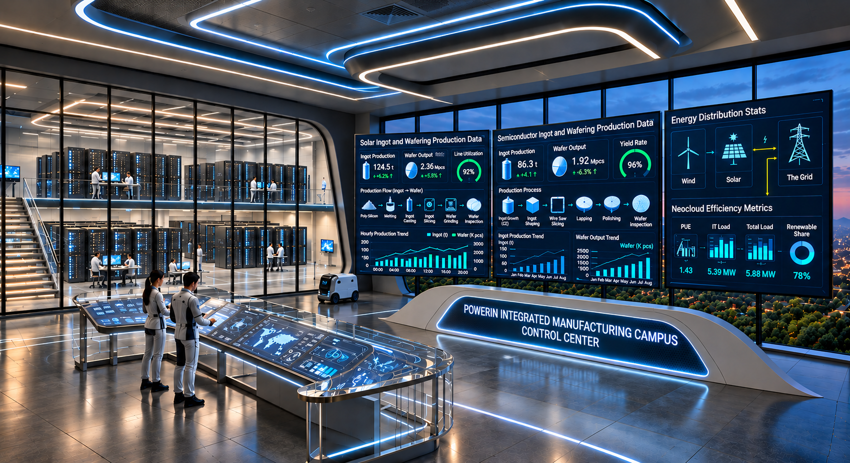
State-of-the-art Czochralski Solar and Semiconductor mono-crystal growth combined with Tungsten-wire wafering.
Solar Product architecture is compatible with PERC / TOPCon / HJT downstream platforms and next-generation tandem applications.
Semiconductor Product architecture is compatible with silicon and silicon carbide wafers.
Technology process flow
N-Type
Designed for advanced solar cell platforms.
Czochralski
Mono-crystal growth process for ingot production.
Tungsten-Wire
Wafering process for precision silicon substrates.
PIMC masterplan
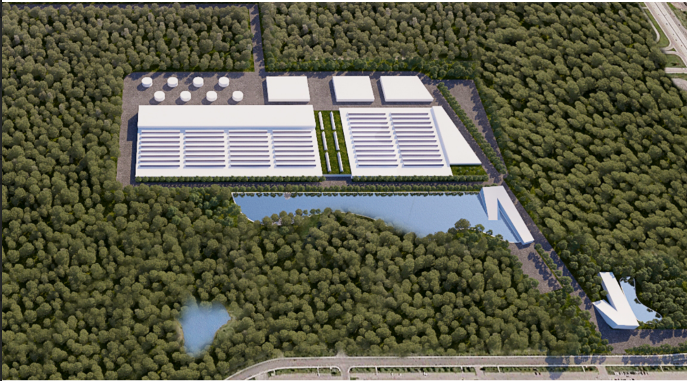
Manufacturing scale- solar
Annual capacity
0 GW
Phase I site
0 acres
Manufacturing scale- semiconductor (pilot line)
Annual capacity
0 wafers
Phase I site
0 acres
Atmanirbhar Bharat lens
Builds domestic upstream capability where the supply chain is structurally import-dependent.
Pairs a non-Chinese polysilicon sourcing strategy with domestic ingot and wafer production.
Creates a base for semiconductor-grade materials, MiniFAB and other advanced device opportunities.
Provides a plug-and-play environment for partners, JVs and captive vendors supporting the campus.
Three-phase campus
Advanced N-Type ingot & wafer production, semiconductor ingot / wafer pilot line and initial energy-storage capability.
Commercial scale semiconductor ingot & wafer platform, semiconductor MiniFAB, expanded ESS and next-generation solar technology.
Hydrogen devices, photonics, mechatronics and additional upstream / advanced manufacturing opportunities.
Strategic roadmap
6 GW, N-Type Ingot + Wafer + Semiconductor pilot line + Neocloud, In execution
Integrated Wafer Manufacturing, Hyper-Pure Polysilicon and critical consumables , miniFAB Strategic direction / subject to execution
Advanced Materials / Semiconductor Optionality, Future optionality
Strategic positioning
Six disciplines of execution
Yield, quality, efficiency
Construction, equipment, commissioning
Equity, debt, working capital
Competitive polysilicon availability
Qualification and long-term offtake
ALMM / PLI / state incentives